










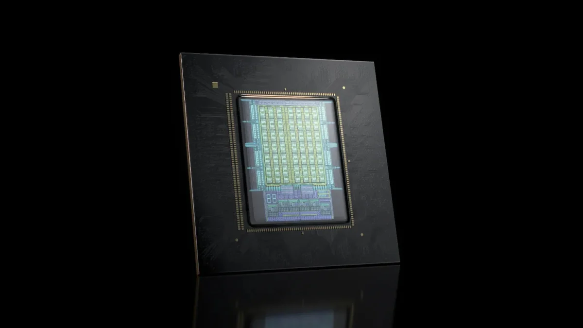
Nvidia has quietly reduced the published memory and interconnect bandwidth specifications for its flagship Vera Rubin AI architecture, lowering per-GPU HBM4 bandwidth by approximately 13% and NVLink speeds by roughly 17%. The stealthy revision, which was executed without a formal press release or direct public announcement, was discovered after eagle-eyed industry observers compared earlier documentation with recently updated product pages. Despite these adjustments to peak theoretical performance metrics, key architectural pillars—such as the headline 50 PFLOPS of sparse NVFP4 inference and the 288 GB memory capacity per GPU—remain unaltered on paper.
The modifications affect several core product tiers across the Rubin lineup, including the Vera Rubin NVL72 rack-scale system, the two-GPU Vera Rubin Superchip, and the widely deployed HGX Rubin NVL8 server boards. While Nvidia has maintained a deliberate silence regarding the underlying engineering reasons for the downclock, the timing of the spec sheet alterations aligns with the hardware’s transition from initial sample distributions to full commercial production. As high-performance computing (HPC) and artificial intelligence infrastructure providers race to deploy next-generation clusters, these subtle specification shifts offer a rare window into the manufacturing and engineering hurdles associated with bleeding-edge memory technologies.
Chronology of the Stealth Revision
The adjustments came to light when technology publication IT Home contrasted Nvidia’s October documentation against archival snapshots captured earlier in the year. Subsequent investigations by Wccftech utilizing the Wayback Machine narrowed the exact revision window to a brief timeframe between September 1 and September 11, 2026. Hardware Busters was among the first to note that Nvidia chose the understated route of directly editing existing product pages rather than issuing a corrective bulletin or briefing reporters.
This silent update arrived at a critical juncture in Nvidia’s deployment cycle. In August 2026, during its second-quarter earnings report, the company confirmed that Vera Rubin racks were already actively operational within partner environments, including CoreWeave, Google Cloud, and Microsoft Azure. These early deployments followed a limited rollout to select enterprise customers earlier in the year, setting the stage for full-scale production shipments promised initially during corporate showcases in mid-2025 and early 2026. Consequently, the newly adjusted figures do not represent distant theoretical goals, but rather the actual physical characteristics of hardware currently rolling off assembly lines and arriving at enterprise data centers.
Detailed Breakdown of Specification Adjustments
A closer examination of the updated product documentation reveals that the performance reduction was not distributed uniformly across all form factors.

On the Vera Rubin NVL72 product page, the HBM4 bandwidth rating for each individual Rubin GPU has been marked down from 22 TB/s to 19.2 TB/s. Simultaneously, NVLink 6 interconnect bandwidth has dropped from 3.6 TB/s down to 3 TB/s. While individual memory capacity stays firm at 288 GB per GPU, the aggregate metrics at the system scale take a noticeable hit. Aggregate memory bandwidth across a full rack drops from 1,580 TB/s to 1,400 TB/s, while the total NVLink bandwidth decreases from 260 TB/s to 216 TB/s. Furthermore, the two-GPU Vera Rubin Superchip sees its combined bandwidth capability fall from 44 TB/s to 38.5 TB/s.
The standard eight-GPU server board, the HGX Rubin NVL8, experienced an even more pronounced downgrade. The official HGX documentation now lists a total system HBM4 allocation of 2 TB delivering 130 TB/s of aggregate bandwidth, down sharply from the previously advertised 2.3 TB and 176 TB/s—marking a substantial 26% reduction in memory bandwidth. Additionally, NVLink Switch bandwidth for the HGX platform fell from 28.8 TB/s to 24 TB/s, while dense training metrics saw minor concessions, dropping from 280 to 270 PFLOPS for NVFP4, and from 140 to 130 PFLOPS for FP8. Interestingly, scale-out networking metrics bucked this downward trend, rising by roughly 12.5% in most configurations, though Nvidia has offered no explanation for this isolated enhancement.
Manufacturing Challenges and Memory Supplier Realities
The technical rationale behind these reductions appears rooted in the complex manufacturing realities of High Bandwidth Memory 4 (HBM4) and the aggressive targets initially set by Nvidia’s product planners.
The JEDEC Solid State Technology Association officially published its HBM4 standard in April 2025, establishing a baseline specification of up to 8 Gb/s per pin across a wide 2,048-bit interface, translating to roughly 2 TB/s per memory stack. However, Nvidia notoriously pushes its component suppliers to the absolute bleeding edge of silicon design. According to industry reports from TechPowerUp and market analysis by TrendForce, Rubin’s per-GPU target evolved rapidly, climbing from an initial 13 TB/s goal at GTC 2025 to 20.5 TB/s by September 2025, and culminating in an ambitious 22 TB/s target announced at CES 2026.
Supply chain intelligence compiled by SemiAnalysis and TrendForce throughout late 2025 and early 2026 highlighted significant friction in meeting these lofty goals. Major memory suppliers—including SK hynix, Samsung, and Micron—grappled with extreme yield and thermal constraints as Nvidia reportedly pressured them to scale speeds from 10 Gbps up to 11 Gbps per pin and beyond. While SK hynix achieved early milestones and Samsung reported shipping high-speed modules in early 2026, the volume production required to sustain a 22 TB/s per-GPU baseline across millions of enterprise units appears to have proved commercially or technically unviable in the immediate term.
By quietly recalibrating its public specifications, Nvidia appears to have adopted a fallback strategy: accepting a slightly lower performance ceiling to ensure predictable hardware delivery schedules and maintain stable manufacturing yields. This pragmatic compromise prioritizes reliable product fulfillment to hyperscale cloud providers over the pursuit of elusive peak marketing metrics.

Competitive Implications and Market Dynamics
The downward adjustment of Vera Rubin’s peak bandwidth specs subtly alters the competitive landscape between Nvidia and its primary rival, Advanced Micro Devices (AMD), particularly within the high-performance AI accelerator market.
AMD approached the HBM4 generation with a different architectural philosophy for its Instinct MI455X accelerators and the Helios rack-scale system launched in July 2026. By distributing 432 GB of memory across 12 HBM4 stacks to achieve 23.3 TB/s of bandwidth, AMD relied on a wider memory interface rather than extreme per-pin signaling speeds. This approach allowed AMD to comfortably operate below the JEDEC baseline speed requirements without putting excessive strain on memory fabrication partners.
When evaluated against Nvidia’s original marketing figures, AMD’s Helios held a competitive baseline, but the revised metrics shift the balance further. Against the updated 1,400 TB/s aggregate rack bandwidth for Vera Rubin NVL72, AMD’s published 1.67 PB/s rack-scale capability positions it approximately 19% ahead in raw memory bandwidth. Furthermore, scale-up interconnect advantages that traditionally favored Nvidia have narrowed, creating a tighter contest for enterprise customers evaluating infrastructure for massive large language model (LLM) training and high-throughput agentic AI inference.
Despite these adjustments, industry analysts emphasize that Vera Rubin remains an extraordinarily powerful architecture. Even at the revised 19.2 TB/s per-GPU specification, the hardware delivers roughly 2.4 times the memory bandwidth of Nvidia’s preceding Blackwell generation, comfortably surpassing older legacy architectures. Furthermore, Nvidia’s overarching marketing claims—such as achieving up to 10 times higher token throughput per megawatt compared to previous generations—remain prominently featured on corporate channels, though company representatives have yet to clarify whether those software-driven efficiency projections were recalculated using the updated hardware figures.
Ultimately, Nvidia’s decision to quietly lower its public specifications underscores the intense engineering pressures governing the modern AI hardware boom. As the industry transitions deeper into the era of agentic AI and massive inference workloads, absolute stability, supply chain predictability, and timely deployment have superseded raw theoretical ceilings as the true currencies of market leadership.