











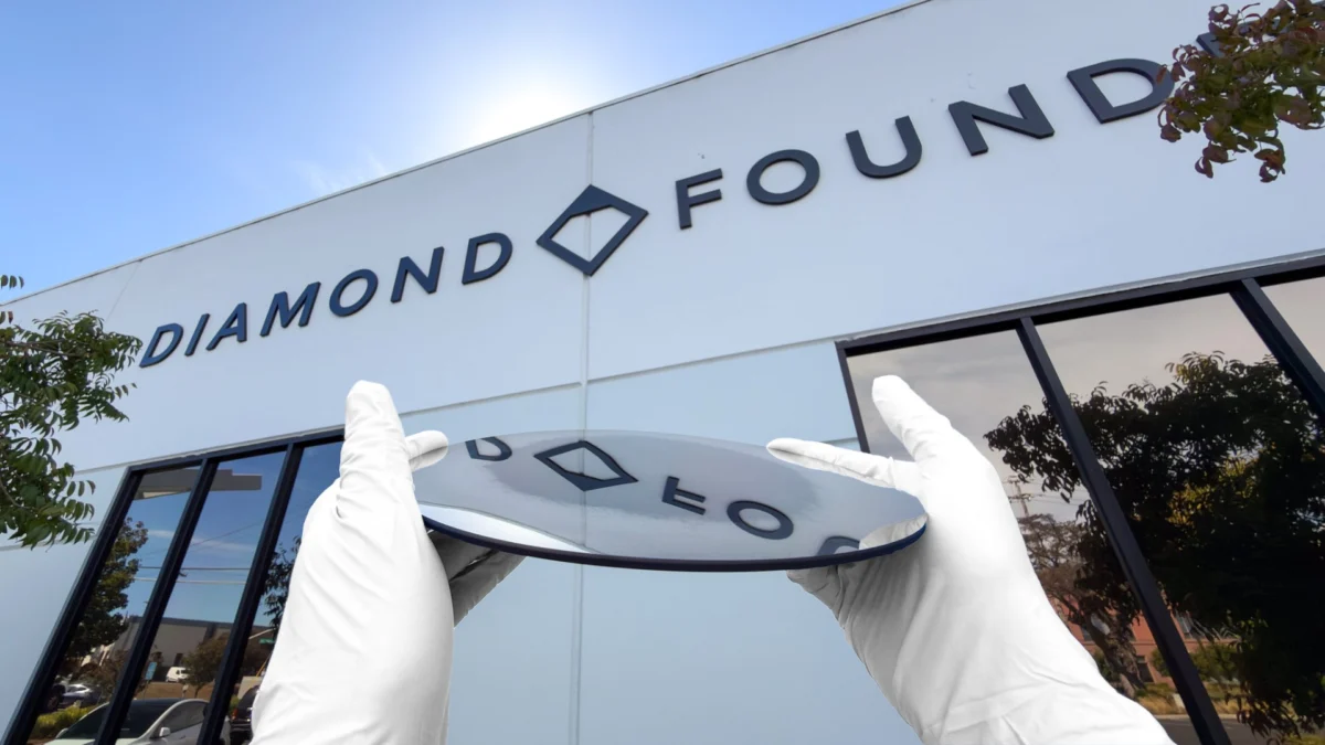
The rapid evolution of high-performance computing and artificial intelligence has pushed traditional thermal management techniques to their absolute limits. As data centers grapple with processors that generate unprecedented amounts of heat, the search for next-generation cooling materials has accelerated across the semiconductor industry. Addressing this critical bottleneck, lab-grown diamond manufacturer Diamond Foundry has officially announced the creation of the world’s first 200mm single-crystal diamond (SCD) wafer. This monumental technical achievement brings diamond-based thermal solutions into the commercial wafer-scale era, offering a material that possesses thermal conductivity at least five times greater than that of copper, the current gold standard in PC and server cooling.
The Main Facts of the Breakthrough
The announcement centers on the successful fabrication of a single-crystal diamond wafer measuring 200 millimeters (approximately 8 inches) in diameter. Historically, synthetic diamonds have been limited to small, discrete plates or fragmentary crystal flakes due to the extreme thermodynamic and kinetic challenges of growing diamond lattices uniformly without defects.
By achieving a 200mm single-crystal format, Diamond Foundry has effectively matched the standard wafer dimensions historically utilized by semiconductor fabrication plants (fabs) for mature manufacturing processes. This dimensional milestone is not merely a geometric victory; it bridges the gap between boutique laboratory material science and mainstream semiconductor manufacturing integration.
Because diamond exhibits exceptional thermal conductivity—typically ranging between 2,000 and 2,200 W/mK at room temperature, compared to copper’s roughly 400 W/mK—it represents the ultimate heat-spreading substrate. Integrating SCD directly into semiconductor packaging or utilizing it as an advanced heat spreader could theoretically eliminate thermal throttling, reduce energy consumption associated with liquid and air cooling, and significantly extend the operational lifespan of power-hungry AI accelerators and GPUs.
Historical Context and Chronology of Diamond Synthesis
To understand the magnitude of this breakthrough, one must examine the painstaking evolution of synthetic diamond production. The journey of growing diamonds in a laboratory began in earnest during the mid-20th century, though early efforts were largely restricted to producing abrasive grits using High-Pressure High-Temperature (HPHT) methods.
In the decades that followed, Chemical Vapor Deposition (CVD) emerged as the preferred method for producing high-purity, electronic-grade single-crystal diamonds. Unlike HPHT, which creates small, blocky crystals under immense mechanical presses, CVD involves feeding hydrocarbon gases—typically methane and hydrogen—into a vacuum chamber and activating them into a plasma. This plasma precipitates carbon atoms layer by layer onto a seed crystal, allowing for greater control over purity and crystalline structure.
For many years, CVD diamond growth was constrained by scalability. Wafers were routinely restricted to square dimensions measuring just a few millimeters or centimeters across. The growth process was plagued by stress fractures, polycrystalline nucleation, and vanishingly slow growth rates.
Over the past ten years, companies like Diamond Foundry scaled up plasma reactor technology, incrementally increasing the surface area capable of maintaining stable single-crystal growth. The transition from sub-inch fragments to a 100mm format represented a major milestone in recent years, but the leap to a full 200mm single-crystal wafer signifies a paradigm shift. By conquering the scaling barrier, the company has positioned SCD to enter the high-volume semiconductor supply chain.
Supporting Data: Thermal Dynamics and the AI Heat Crisis
The timing of Diamond Foundry’s announcement aligns precisely with a structural crisis in the tech industry: the thermal wall hit by modern silicon. Modern artificial intelligence hardware, ranging from hyperscale training clusters to high-end enterprise accelerators, regularly feature thermal design power (TDP) envelopes exceeding 500 to 1,000 watts per socket.
Traditional cooling methodologies—including aluminum and copper heatsinks, vapor chambers, and complex closed-loop liquid cooling systems—are increasingly struggling to dissipate localized heat fluxes (hot spots) on monolithic and multi-chiplet silicon dies. When heat cannot be drawn away from the silicon die instantaneously, processors undergo thermal throttling, deliberately slowing down clock speeds to prevent physical destruction of the semiconductor junctions.
Copper, while ductile, abundant, and possessing a thermal conductivity of roughly 380 to 400 W/mK, pales in comparison to diamond. Pure single-crystal diamond transfers heat at speeds up to five times faster than copper. Furthermore, diamond boasts an exceptionally low thermal expansion coefficient and high electrical insulation properties (when un-doped), making it an ideal substrate for direct-die cooling and three-dimensional (3D) integrated circuit stacking.
By utilizing a 200mm wafer format, chip designers and packaging engineers can process thousands of diamond-based heat spreaders or substrate layers using standard semiconductor lithography and dicing equipment. This compatibility with existing fab infrastructure is critical for commercial viability; a revolutionary material is rarely adopted if it requires entirely new, custom-built industrial ecosystems from the ground up.
Industry Implications and Market Reactions
While Diamond Foundry’s public declaration has generated considerable enthusiasm among semiconductor packaging engineers and high-performance computing (HPC) architects, industry analysts emphasize that commercial integration will require rigorous testing, reliability validation, and cost optimization.
The economic hurdle has historically been the primary obstacle to diamond adoption in consumer and enterprise hardware. Lab-grown diamonds require vast amounts of energy, specialized equipment, and extended growth cycles. However, as the total cost of ownership for AI data centers skyrockets—driven largely by the electricity consumed by cooling infrastructure and HVAC systems—the return on investment for ultra-efficient thermal management materials becomes increasingly justifiable. Hyperscale data center operators, such as Microsoft, Google, Amazon, and Meta, are heavily incentivized to invest in hardware solutions that reduce thermal resistance and improve power efficiency.
Furthermore, the defense, aerospace, and electric vehicle (EV) sectors stand to benefit immensely. Wide-bandgap semiconductors based on gallium nitride (GaN) and silicon carbide (SiC) generate intense thermal densities in tight physical spaces. Pairing these power electronics with diamond substrates could yield unprecedented power density improvements for EV traction inverters and radar systems.
Broader Impact on the Future of Computing
The introduction of the 200mm single-crystal diamond wafer marks a symbolic and practical turning point for materials science in the digital age. As Moore’s Law slows down, the industry has increasingly relied on advanced packaging, heterogeneous integration, and novel materials to sustain performance gains.
Thermal management is no longer merely an auxiliary engineering concern; it is the primary governing factor determining whether next-generation AI models can be trained and deployed efficiently. By successfully scaling diamond synthesis to semiconductor-grade dimensions, Diamond Foundry has unlocked a foundational material that could redefine thermal architecture for the next several decades.
As the engineering community awaits further technical disclosures regarding yield rates, doping capabilities, and pricing structures, the message from the laboratory is definitive: the diamond age of semiconductor cooling has officially arrived.