

NEO Semiconductor, a company at the forefront of memory innovation, announced on April 23rd the successful proof-of-concept (POC) validation of its groundbreaking 3D X-DRAM technology. This pivotal development demonstrates the feasibility of manufacturing a new class of high-density Dynamic Random Access Memory (DRAM) by leveraging existing 3D NAND flash memory infrastructure. The announcement was further bolstered by news of a strategic investment led by Stan Shih, the venerable founder and former Chairman and CEO of Acer, who also served as a board director of TSMC for over two decades, lending significant credibility and industry gravitas to NEO Semiconductor’s ambitious vision.
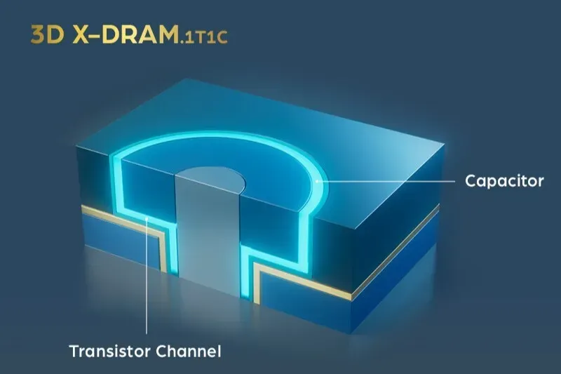
The core of this significant announcement revolves around NEO Semiconductor’s 3D X-DRAM technology, which aims to transcend the conventional scaling limitations currently facing traditional DRAM. By adopting a vertically stacked architecture, akin to how 3D NAND revolutionized flash memory, 3D X-DRAM promises substantial advancements in memory density, energy efficiency, and overall performance, making it particularly well-suited for the increasingly demanding requirements of artificial intelligence (AI) and machine learning workloads. This vertical integration represents a fundamental departure from the planar (2D) scaling methods that have driven DRAM advancements for decades, which are now approaching fundamental physical limits.
The Critical Need for Next-Generation Memory
The semiconductor industry is currently grappling with a pressing challenge: the widening gap between computational power and memory bandwidth, especially in the context of AI. Over the past decade, advancements in Graphics Processing Units (GPUs) and specialized AI accelerators have led to an exponential increase in processing capabilities. However, the rate at which data can be fed to these powerful processors – known as memory bandwidth – has struggled to keep pace. This bottleneck severely limits the efficiency and performance of large-scale AI training, inference, and data analytics systems, impacting everything from large language models (LLMs) to complex scientific simulations.
Traditional DRAM, while continually optimized, faces inherent physical constraints in its 2D architecture. Shrinking transistor sizes in a planar fashion leads to increased leakage current, higher power consumption, and diminishing returns in terms of density and performance gains. The industry has already responded with solutions like High-Bandwidth Memory (HBM), which vertically stacks multiple finished DRAM dies and connects them with Through-Silicon Vias (TSVs) to achieve significantly higher bandwidth. While effective, HBM manufacturing is complex, requires specialized stacking and bonding processes, and comes with a higher cost per bit. The search for more scalable, cost-effective, and higher-density memory solutions is therefore paramount, driving companies like NEO Semiconductor to explore radical new architectures.
Unpacking the Proof-of-Concept Validation
The successful proof-of-concept chips were meticulously fabricated and tested at Taiwan’s National Institutes of Applied Research – Taiwan Semiconductor Research Institute (NIAR-TSRI) in close collaboration with National Yang Ming Chiao Tung University (NYCU). These institutions provided a robust environment for rigorous evaluation, ensuring the results were scientifically sound and technically verifiable. The validation process yielded impressive performance metrics that underscore the potential of 3D X-DRAM:
- Read/Write Latency: Achieved under 10 nanoseconds. This is a crucial metric for DRAM, indicating quick access times which are essential for high-performance computing and AI applications where data must be retrieved and stored rapidly.
- Data Retention: Demonstrated over 1 second at 85°C (185°F). This figure represents a claimed 15-fold improvement over the JEDEC (Joint Electron Device Engineering Council) standard for DRAM, which typically specifies retention in milliseconds. Extended data retention is vital for memory reliability, especially in enterprise-grade servers and data centers, reducing the frequency of refresh cycles and thus lowering power consumption.
- Bit-line Disturbance: Maintained stability for over 1 second at 85°C (185°F). Bit-line disturbance refers to unwanted voltage fluctuations in adjacent memory cells during read/write operations. Superior resistance to disturbance ensures data integrity and operational stability.
- Word-line Disturbance: Similarly, showed stability for over 1 second at 85°C (185°F). Word-line disturbance relates to interference affecting cells connected to the same word line. Robustness against this ensures consistent performance across the memory array.
- Endurance: Achieved greater than 10^7 cycles. Endurance measures how many times a memory cell can be programmed and erased before failure. A high endurance rating is critical for long-term reliability and suitability in applications with frequent data writes, such as caching or persistent memory functions.
These results, particularly the exceptional data retention and disturbance resistance at elevated temperatures, signify a strong foundation for the technology’s reliability and its potential to operate efficiently in demanding environments.
The Strategic Advantage: Leveraging 3D NAND Infrastructure
One of the most compelling aspects of NEO Semiconductor’s announcement is the claim that 3D X-DRAM can be manufactured using existing 3D NAND infrastructure. This is a game-changer for several reasons:
- Cost-Effectiveness: Building new fabrication facilities (fabs) for novel memory technologies is incredibly capital-intensive, often costing tens of billions of dollars. By adapting existing 3D NAND fabs, manufacturers can significantly reduce initial investment costs and accelerate time-to-market. The semiconductor industry has invested heavily in 3D NAND production lines over the last decade, developing mature processes for vertical stacking, advanced etching, and deposition.
- Faster Adoption: The learning curve for manufacturing 3D NAND is already well-established. Leveraging these proven processes and equipment allows for a smoother transition to mass production compared to developing entirely new manufacturing techniques from scratch. This could potentially shorten the notoriously long development cycles for new memory types.
- Scalability: 3D NAND technology is designed for high-volume manufacturing of vertically stacked structures. Applying this expertise to DRAM offers a clear path to achieving the ultra-high densities required for future computing, potentially offering capacities far exceeding current HBM or DDR modules. The distinction here is critical: while HBM stacks finished dies, 3D X-DRAM aims for a monolithic vertical structure where memory cells are fabricated in layers as part of the memory array itself, similar to how 3D NAND builds up its storage cells. This fundamental difference could lead to greater integration density and potentially lower per-bit costs at scale.
Industry Commentary and Investor Confidence
The positive industry commentary included in NEO Semiconductor’s announcement further underscores the significance of this breakthrough. Jeongdong Choe, a respected analyst at TechInsights, characterized the results as a "significant milestone" in the industry’s shift towards 3D memory architectures. Choe’s observation highlights the widely acknowledged reality that conventional planar DRAM scaling is rapidly approaching its physical limits. As such, the exploration of vertical alternatives is not merely an academic exercise but a strategic imperative for the entire memory industry.
The strategic investment led by Stan Shih provides more than just capital; it offers invaluable validation and strategic guidance. Shih’s long and distinguished career, encompassing the founding of Acer (a global computing giant) and decades of service on TSMC’s board, gives him unparalleled insight into the semiconductor manufacturing landscape, market dynamics, and technological trends. His backing suggests a strong belief in NEO Semiconductor’s technology and its potential to disrupt the memory market, signaling to other potential investors and industry partners that 3D X-DRAM is a technology worth serious consideration.

The Broader Landscape of AI Memory Solutions
NEO Semiconductor’s 3D X-DRAM is not operating in a vacuum. The intense demand for AI memory has spurred innovation across the industry, leading to multiple approaches to address the bandwidth and capacity challenges. Just a day prior to NEO Semiconductor’s announcement, news emerged about SAIMEMORY and its ZAM (Zero-capacitor Access Memory) architecture. Backed by SoftBank and Intel, and receiving crucial support from the Japanese government, SAIMEMORY is also pursuing novel memory designs aimed at providing a lower-power alternative to HBM for AI workloads.
Other research initiatives are exploring emerging memory technologies such as Resistive RAM (RRAM), Phase-Change Memory (PCM), and Magnetoresistive RAM (MRAM), all of which offer different combinations of speed, density, and non-volatility. Each of these technologies presents unique advantages and challenges in terms of manufacturability, cost, and integration into existing systems. The competitive landscape underscores the urgency and the significant market opportunity for a scalable, high-performance memory solution that can effectively meet the future demands of AI.
Challenges and Future Implications
While the successful proof-of-concept validation is a monumental step, it is crucial to temper enthusiasm with the understanding that the journey from lab validation to commercial volume production is long and fraught with challenges. The history of the semiconductor industry is "littered with the remains of promising memory technologies that never made it out of the lab" – a testament to the immense complexities involved in scaling production, ensuring yield, and achieving cost-effectiveness at a mass market level.
However, NEO Semiconductor’s emphasis on utilizing established 3D NAND processes provides a distinct advantage. This approach mitigates some of the most formidable hurdles typically associated with bringing entirely new memory architectures to market. The next phases for NEO Semiconductor will likely involve:
- Further Development and Optimization: Refining the manufacturing process, optimizing cell design, and integrating the technology with controller logic.
- Pilot Production: Establishing small-scale pilot lines to demonstrate manufacturing yields and consistency.
- Industry Partnerships: Collaborating with major memory manufacturers (e.g., Samsung, SK Hynix, Micron) or foundry services to scale production and integrate 3D X-DRAM into their product portfolios. Given the massive capital expenditures required for memory fabrication, such partnerships are almost always essential for commercial success.
- Standardization: Working with industry bodies like JEDEC to establish standards for 3D X-DRAM, which is critical for broad market adoption.
The potential implications of 3D X-DRAM reaching commercial viability are profound. It could lead to:
- Revolutionized AI Hardware: Enabling significantly denser and more power-efficient memory modules for AI accelerators, allowing for larger models, faster training, and more sophisticated edge AI applications.
- Enhanced Data Center Performance: Boosting the overall performance and energy efficiency of cloud computing infrastructure, crucial for the massive data processing demands of the digital age.
- Cost Reductions: Potentially driving down the cost per bit for high-density DRAM, making advanced computing more accessible.
- New Computing Paradigms: Opening doors for novel computing architectures that rely on vast amounts of fast, integrated memory, such as in-memory computing or near-memory processing.
Jack Sun, Senior Vice President of NYCU and Dean of IAIS, and former CTO of TSMC, succinctly captured the essence of this achievement: "The successful proof-of-concept not only demonstrates the potential of innovative memory architectures, but also confirms the feasibility of implementing advanced memory technologies using mature processes. This collaboration among NEO, NYCU IAIS, and NIAR-TSRI further underscores the value of industry–academia partnerships in accelerating innovation from concept to practical implementation." His statement highlights the critical role of synergistic collaborations between academic research and industrial innovation in driving forward the frontiers of technology.
In conclusion, NEO Semiconductor’s 3D X-DRAM validation marks a significant step forward in the quest for next-generation memory. By offering a path to higher density, lower power, and manufacturability through existing infrastructure, it presents a compelling vision for overcoming the AI memory bottleneck. While the journey to mass production is undoubtedly challenging, the foundational technical achievements and strategic industry backing position 3D X-DRAM as a leading contender in the race to power the future of computing.


