

The semiconductor manufacturing landscape has reached a significant watershed moment as Intel Foundry and Dutch lithography giant ASML jointly announced that they have successfully processed over one million 300mm wafers utilizing ASML’s cutting-edge High-Numerical Aperture Extreme Ultraviolet (High-NA EUV) lithography scanners. The announcement, made during the prestigious SPIE Photomask Technology and EUV Lithography conference held in Monterey, California, highlights a major technological leap for Intel. Once viewed as an underdog struggling to keep pace in the hyper-competitive artificial intelligence hardware and semiconductor foundry markets, Intel is steadily cementing its status as an aggressive pioneer in advanced node manufacturing.
This hard-won milestone arrives at a time of dramatic corporate transformation for Intel. Following a challenging period marked by delayed product roadmaps, skepticism regarding its foundry ambitions, and a perceived lag behind AI accelerator giants like Nvidia, the company has engineered a notable resurgence. Intel’s stock price has rallied impressively, surging nearly 155% year-to-date, buoyed by strategic partnerships, increased institutional confidence, and targeted investments from key industry players and the United States government—all eager to secure domestic access to advanced semiconductor manufacturing capabilities.
Deconstructing the One Million Wafer Milestone
To properly contextualize the significance of processing one million wafers, industry analysts emphasize the need to look closely at what the metric actually entails. According to the joint press disclosure released by Intel and ASML, the one-million-wafer figure is a cumulative total that encompasses various stages of development. Specifically, it includes intensive internal research and development (R&D) projects, complex tool certification runs, and early volume production metrics for Intel’s upcoming Core Ultra Series 3 central processing units, widely recognized under the code name Panther Lake.
Consequently, industry observers caution that this figure should not be interpreted as one million commercially shipping, retail-grade Panther Lake consumer chips ready for immediate market deployment. Neither Intel nor ASML has released granular commercial production volumes for specific consumer silicon lines. Nevertheless, within the context of semiconductor manufacturing, pushing one million wafers through a novel, highly complex lithography platform is an extraordinary engineering feat.
The scale of Intel’s achievement becomes even clearer when evaluated against ASML’s broader deployment data. Greet Storms, ASML’s head of High-NA product management, recently reported that the company’s EXE-series systems have collectively exposed more than 1.35 million wafers globally. With approximately ten High-NA systems currently operational across four major semiconductor clients—alongside three additional units currently in the pipeline for shipping or installation—Intel’s individual output accounts for roughly 74% of all High-NA wafer exposures globally. This places Intel far ahead of other heavyweights in the semiconductor foundry space, a roster that includes foundry titan TSMC, South Korean memory and logic giant Samsung, and memory specialist SK Hynix.
A High-Stakes Gamble on First-Mover Advantage
The financial and operational implications of this milestone are substantial for institutional investors and technology analysts alike. Intel currently holds an undisputed, lonely lead in the commercial adoption of High-NA EUV technology. While competitors tread cautiously, carefully weighing the astronomical capital expenditures required to transition to the new toolsets, Intel has essentially bet its foundry future on being the first mover.
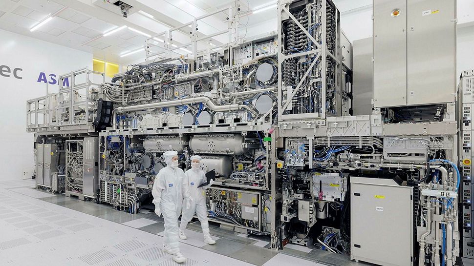
Each individual High-NA EUV machine carries a staggering price tag of approximately $350 million. Acquiring, delivering, and commissioning these colossal machines requires years of meticulous facility preparation, with lead times stretching up to six years. For Intel, which aggressively committed capital to secure these systems early, the strategy was designed to leapfrog traditional scaling limitations and secure process node dominance.
By contrast, rival foundries are taking a more measured approach. TSMC, for instance, has publicly indicated that it does not plan to transition to High-NA EUV for high-volume commercial manufacturing until closer to 2030, preferring to extract maximum yield and value from its existing Low-NA EUV (0.33 NA) toolsets before absorbing the immense costs associated with the newer 0.55 NA systems. While this conservative approach mitigates early capital risk for TSMC, it risks ceding technological leadership in sub-nanometer scaling to Intel if the American manufacturer can successfully stabilize and monetize its High-NA manufacturing lines at scale.
The Evolution of Lithography: From Low-NA to High-NA EUV
To understand the magnitude of processing one million wafers on High-NA equipment, one must examine the technological evolution of photolithography. For decades, the semiconductor industry relied on optical lithography, eventually transitioning to Deep Ultraviolet (DUV) light sources. However, as transistor features shrank below the 10-nanometer threshold, traditional light wavelengths proved insufficient to print the incredibly minute circuits required for modern computing.
This necessitated the introduction of Extreme Ultraviolet (EUV) lithography, utilizing a 13.5-nanometer wavelength generated by vaporizing microscopic droplets of tin with high-powered lasers inside a vacuum chamber. Standard Low-NA EUV systems utilized a numerical aperture of 0.33, which successfully guided the industry through the production of advanced nodes down to the 3nm and 2nm eras. However, as chip designers target sub-2nm architectures and gate-all-around (GAA) transistor designs, optical diffraction limits once again begin to degrade pattern fidelity.
High-NA EUV introduces a numerical aperture of 0.55, significantly increasing the light-gathering and focusing power of the system’s massive, highly polished anamorphic mirrors. This advancement allows for sharper resolution, enabling chipmakers to print finer features in a single exposure step rather than resorting to complex multi-patterning techniques. Multi-patterning—splitting a single circuit layer across multiple exposures—drastically increases manufacturing cycle times, introduces alignment errors, and drives up production costs. By executing single-exposure patterning for critical layers, High-NA EUV promises to streamline manufacturing workflows, improve chip yields, and accelerate time-to-market for next-generation processors.
Chronology of Intel’s High-NA Journey
The path to reaching one million High-NA wafers has been a multi-year endeavor defined by intensive engineering collaboration between Intel and ASML:
- Late 2023 / Early 2024: Intel receives the world’s first commercial High-NA EUV system (the ASML Twinscan EXE:5000) at its development fab in Hillsboro, Oregon. The massive machine, delivered in parts via cargo planes, marks the physical commencement of the High-NA era.
- Mid 2024: Engineers spend months assembling, calibrating, and aligning the optical systems. Due to the extreme precision required, even microscopic vibrations or thermal fluctuations can disrupt the machine, making tool calibration a monumental scientific challenge.
- Late 2024 to 2025: Intel achieves "first light" and begins successfully printing test patterns. The focus shifts toward mask optimization, pellicle development (protective membranes that shield photomasks from debris), and photoresist chemistry adjustments tailored specifically for the 0.55 NA light cone.
- 2026: Intel transitions the toolsets from pure R&D environments toward tool certification runs and integration into active production workflows, culminating in the recent announcement at the Monterey SPIE conference that cumulative wafer processing has officially crossed the one-million mark, largely driven by work on the Panther Lake platform.
Industry Reactions and Competitive Dynamics
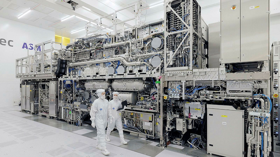
The reaction from the broader semiconductor ecosystem to Intel’s milestone has been a mix of cautious admiration and professional skepticism. Industry analysts point out that while a cumulative total of one million wafers is an impressive operational milestone, the true test of High-NA EUV lies in its economic viability and defect density at mass production scale.
Rival foundries like TSMC and Samsung continue to monitor Intel’s progress closely. Because Intel Foundry operates both as an internal manufacturer for its own client products and as an external foundry for third-party chip designers, its success with High-NA tools serves as a live-fire testbed for the entire industry. If Intel can demonstrate high yields, acceptable cost-per-wafer metrics, and reliable tool uptime, it could compel competing foundries to accelerate their own High-NA adoption timelines to avoid being left behind.
Conversely, skeptics argue that the extreme cost of ownership for High-NA equipment could pressure Intel’s operating margins. With each machine costing upwards of $350 million—coupled with expensive peripheral infrastructure, specialized resists, and dedicated cleanroom modifications—the financial hurdle to achieve a return on investment is extraordinarily high. Intel must secure a robust roster of external foundry customers willing to pay premium prices for wafers produced on the bleeding-edge node to offset these capital expenditures.
Broader Economic and Geopolitical Implications
Beyond corporate balance sheets, Intel’s heavy investment in High-NA EUV carries profound geopolitical significance. In an era where semiconductor manufacturing is viewed as critical national security infrastructure, the United States government has placed immense strategic importance on revitalizing domestic chip production.
Through legislative frameworks such as the CHIPS and Science Act, Washington has sought to reduce American reliance on concentrated Asian supply chains, particularly in Taiwan and South Korea. Intel remains the primary domestic champion capable of producing leading-edge logic semiconductors on American soil. By successfully pushing the envelope in High-NA EUV technology within its Oregon and Ohio facilities, Intel not only secures its own technological roadmap but also ensures that the United States maintains a vital foothold at the absolute frontier of microelectronics manufacturing.
Looking Ahead: The Road to Commercialization
As Intel and ASML look past the one-million-wafer milestone, the immediate focus shifts toward the refinement of high-volume manufacturing (HVM) processes. The insights gathered from processing millions of experimental and pre-production wafers have provided both companies with invaluable data regarding tool reliability, lens degradation, beam source stability, and chemical interactions.
For consumers and enterprise technology buyers, the payoff of this colossal manufacturing gamble will manifest in the coming years. As Panther Lake and subsequent processor generations scale toward full commercial availability, they will serve as the tangible proof of concept for whether High-NA EUV can deliver on its promise of denser, faster, and more energy-efficient computing hardware. For now, Intel has proven that it is willing to make bold, expensive bets to reclaim its technological crown—and in doing so, it has pushed the entire global semiconductor industry one step closer to the future of manufacturing.